In semiconductor fabs, every wafer matters. Even a single microscopic defect can compromise chip performance, leading to millions of dollars in losses if issues go undetected. Traditional wafer defect classification methods, often dependent on manual inspection or rigid rule-based systems, are no longer enough for today’s advanced fabrication processes. They are slow, inconsistent, and prone to human error.
This is exactly where Agentic AI systems provide a breakthrough. By combining autonomous decision-making with real-time defect detection, these solutions offer fabs a way to dramatically improve accuracy, speed, and cost efficiency.
At Theta Technolabs, we focus on building solutions that don’t just analyze data—they act. Our approach to wafer defect classification automation is centered on solving the core problems fabs face: yield loss, operational inefficiencies, and unpredictable costs.
Why Traditional Approaches Fail
Most fabs rely on manual classification supported by rule-based software. The problem is that wafers are becoming more complex, and defect patterns no longer follow predictable rules. Human operators can miss subtle anomalies. Rule-based systems cannot keep up with evolving chip designs.
The result? High scrap rates, lower yield, and reduced profitability.
Agentic AI offers a way out of this cycle by continuously learning, adapting, and improving classification decisions.
The Agentic AI Solution
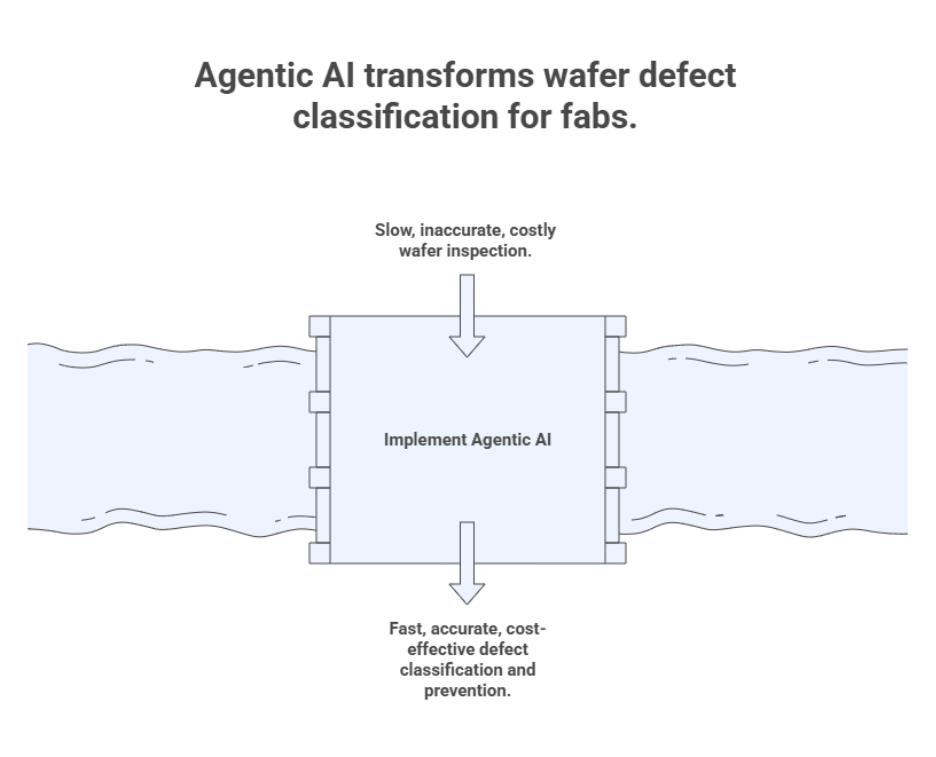
Our solution-centric model for wafer defect classification uses Agentic AI to deliver outcomes that fabs can measure in speed, accuracy, and cost savings.
1. Automated Defect Detection and Classification
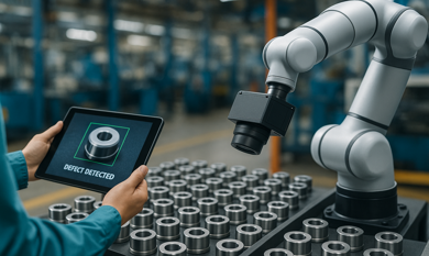
Instead of relying on static rules, our Agentic AI models use deep learning and computer vision to identify particles, scratches, cracks, and material inconsistencies with unmatched accuracy. The system classifies defects in real time, ensuring no defective wafer goes unnoticed.
2. Adaptive Learning That Improves Over Time
As more wafers are processed, the system learns from each classification. Unlike legacy systems, this AI does not require extensive reprogramming to adapt to new designs. It becomes more intelligent with use, which means fabs gain a solution that evolves alongside their manufacturing processes.
3. Real-Time Decision-Making
Agentic AI is not just about defect detection—it is about deciding the next best action. Whether a wafer needs rework, further inspection, or immediate rejection, the system acts instantly. This reduces delays and prevents costly bottlenecks.
4. Seamless Fab Integration
Theta Technolabs’ AI-driven solutions are designed for smooth integration with Manufacturing Execution Systems (MES) and existing fab tools. That means fabs don’t need to reinvent their infrastructure to adopt AI automation.
5. Actionable Insights Beyond Classification
Every wafer inspection is also a source of insight. Our solutions capture defect trends, highlight recurring issues, and give fabs the intelligence to improve upstream processes, reducing the probability of future defects.
Business Impact: What Fabs Gain
Implementing an Agentic AI solution for wafer defect classification transforms fab operations in measurable ways:
- Higher Yield: More usable chips per wafer thanks to precise defect identification.
- Reduced Scrap and Waste: Early detection minimizes unnecessary processing of defective wafers.
- Lower Operational Costs: Less manual inspection, fewer errors, and reduced downtime.
- Faster Time-to-Market: Automated classification accelerates production cycles.
- Consistent Quality: Uniform AI-driven decisions eliminate human variability.
This is not just about improving a single process. It is about reshaping the economics of semiconductor manufacturing.
Overcoming the Challenges
Fabs often ask: “Is AI adoption worth the investment?”
The short answer: Yes, when the solution is tailored for your environment.
At Theta Technolabs, we address the common barriers to adoption:
- Data Availability: We help fabs structure defect image datasets and apply transfer learning to minimize training time.
- Integration Costs: Our solutions are modular, ensuring cost-effective deployment without full system replacement.
- Change Management: We provide training and support so teams can confidently work alongside Agentic AI.
- Security Concerns: Data protection is built into every layer of our AI solutions.
By focusing on outcomes, we ensure fabs see ROI quickly, often within the first production cycles.
Experience and Expertise That Build Trust
Theta Technolabs has deep experience in Web, Mobile, and Cloud solutions, but our expertise extends into designing AI systems that solve industry-specific challenges. With semiconductor fabs, we apply a practical, outcome-first approach to automation.
Our authority comes not only from building AI tools but from implementing solutions that drive measurable business results. We understand that wafer defect classification is mission critical. That’s why we design systems that fabs can rely on with confidence.
Trust is built on results, and our Agentic AI solutions deliver consistent, repeatable outcomes that align with fabs’ business goals.
Tailored Solutions for Semiconductor Startups and Enterprises
Not all fabs have the same requirements. Some need fully automated classification, while others prefer hybrid systems where AI augments human expertise. Theta Technolabs provides flexibility by tailoring solutions based on fab size, complexity, and long-term goals.
This is particularly important for semiconductor startups that want to scale without massive upfront costs. Here, Agentic AI development services, startup IT solutions & services Dallas come into play, helping smaller fabs access world-class AI capabilities at a fraction of traditional investment.
Looking Ahead: The Future of Agentic AI in Fabs
Agentic AI will continue to evolve, making wafer defect classification even more powerful through:
- Explainable AI: Giving fabs visibility into how classification decisions are made.
- Edge AI Processing: Embedding intelligence directly into inspection machines for instant results.
- Collaborative AI: Combining human oversight with AI precision for maximum confidence.
- Cross-Fab Data Sharing: Enabling industry-wide learning while preserving proprietary data.
The fabs that embrace these solutions early will not just cut costs but will set themselves apart as leaders in efficiency and quality.
Conclusion
The pressure on semiconductor fabs is higher than ever. The solution is not to add more manual checks or rules but to adopt systems that can think, act, and adapt. Agentic AI does exactly that by automating wafer defect classification and ensuring every wafer is evaluated with speed and precision.
Theta Technolabs is a trusted technology partner specializing in Web, Mobile, and Cloud solutions. As an Agentic AI development company Dallas, we bring deep expertise in designing AI systems that deliver tangible results for semiconductor fabs.
If your fab is ready to embrace the future of wafer defect classification, our team is here to help you take the next step.
📩 Contact us at sales@thetatechnolabs.com and discover how Agentic AI can redefine your manufacturing outcomes.
Ready to Automate Wafer Defect Classification with Agentic AI?
Email sales@thetatechnolabs.com today and partner with Theta Technolabs to implement AI-driven solutions that improve yield, reduce costs, and accelerate production cycles.




.png)


.png)


.png)


.png)








.png)
.png)




.png)

.png)
.png)
.png)


.png)
.png)
.png)
.png)


